Lesson 4: Photovoltaics
Overview
Overview
This lesson contains materials describing the main principles of photovoltaic conversion of light. You will learn what properties of PV materials determine the performance of the solar cells, and how that performance is measured. You should be able to look at the performance curve and say if it is good or not, if you deal with a single cell or a module. We will also see what happens to the parameters of the PV actions on system scale-up. Different types of PV materials and systems will be discussed here, and recent innovations and trends to improve solar cell efficiency will be reviewed.
Learning Outcomes
By the end of this lesson, you should be able to:
- understand and explain the principle of photovoltaic effect;
- analyze the photovoltaic cell performance data;
- discuss innovative ideas and recent trend in PV development.
Readings
Duffie, J.A. and Beckman, W.A., Solar Engineering of Thermal Processes, 4th Ed., John Wiley and Sons, 2013. Parts of Chapters 2 and 7. Please refer to particular sections of the lesson for more specific assignment.
Honsberg, C and Bowden, S., Photovoltaic Education Network [1], Accessed: May 2020.
Kalogirou, S.A., Solar Energy Engineering. Processes and Systems. Elsevier, 2009, Chapter 9. Photovoltaic Systems, pp. 483-486.
4.1 Photovoltaic effect
4.1 Photovoltaic effect
The word "photovoltaic" immediately indicates the connection between light (phot- greek) and electricity (volt, unit for electric potential). The key property of a photovoltaic material is to convert light energy to electric current. This conversion takes place due to the photovoltaic effect - a physical phenomenon in a semiconductor, which we are going to discuss next.
Semiconductors are a special class of materials, whose conductance is not permanent, but rather depends on the energy available to activate electrons in the crystal lattice. Crystalline silicon is a semiconductor material widely used in photovoltaics. It becomes conductive when the energy of the photons absorbed by the crystal surface is sufficient to raise the electron state from the valence band to the conduction band. This required amount of energy to excite an electron is defined as band gap. Band gap is an intrinsic property of semiconductors and eventually has a direct influence on the photovoltaic cell voltage. The following schematic (Figure 4.1) provides a demonstration of the band gap concept.

In this picture, we can visualize the difference between different classes of materials: conductors (metals), semiconductors, and insulators. The valence and conduction bands in a metal overlap, so it does not take any significant energy to free the electrons. They are available for conduction as soon as the potential gradient is provided. In insulators, the gap between the valence and conduction bands is very large, so it requires so much energy to free the electrons that it can damage the material itself. For semiconductors, the situation is somewhere in between. The band gap is big enough to prevent spontaneous conduction and to provide separation of charges, and small enough to be matched by photon energy.
The band gap energies of several different materials are listed in Table 4.1 below. Some of those materials are more suitable for photovoltaic applications than others. How suitable the materials are for photovoltaic applications would be determined by how close the photon energy is to the band gap of the material, and if the energy of photon is sufficient to cover the band gap.
| Material | Band Gap (eV) | |
|---|---|---|
| Si | Silicon | 1.11 |
| Ge | Germanium | 0.67 |
| CdTe | Cadmium telluride | 1.5 |
| Cu2O | Copper oxide | 2.1 |
| Cu3N | Copper nitride | 1.75 |
| GaP | Gallium phosphide | 2.26 |
| GaAs | Gallium arsenide | 1.43 |
| PbS | Lead sulfide | 0.37 |
| Si3N4 | Silicon nitride | 5 |
| C | Diamond | 5.5 |
| SiO2 | Silica | 9 |
For example, if we have a photon with energy of 2 eV hitting silicon surface, 1.1 eV of that energy will be used to move an electron to the conduction band; the rest of the energy (0.9 eV) will be dissipated as heat. However, if a material with a greater band gap is used, for instance copper oxide, 2 eV is not enough to free the electron. We would need a higher energy photon there.
By the way, you may remember from physics that photon energy is dependent on the wavelength of light. The shorter the wavelength (λ), the higher the frequency of the light (ν), and the more energy it brings:
(where h is the Plank constant, and C is the speed of light)
For instance, for the red side of the visible light spectrum, , so we can find:
At the same time, for the violet side of the visible spectrum, , and:
Obviously, the photons associated with high frequency radiation (violet, UV) deliver more energy and can be used with larger band gap materials.
Check this out
Photon energy calculator from the PVEducation website. [4]
Check the numbers given in the above example. You may also want to see what light wavelengths would be suitable for the materials listed in Table 4.1.
Based on these reflections, we see that low band gap materials (such as germanium), can be used to capture low energy photons (like those in the red and IR parts of the spectrum), and high band gap materials (e.g. copper nitride or gallium phosphide) can be used for using high energy photons. Combination of different materials in one system allows for more efficient use of available radiation. At the same time, if the band gap of the PV material is too small compared to the incident photon energy, a significant amount of energy will be converted to heat, which is not a good thing for PV cell itself. No matter how much higher the photon energy is compared to the band gap, only one electron can be freed by one photon. This is the reason for the limited efficiency of the photovoltaic cells.
The data in Figure 4.2 show how the maximum efficiency of a solar cell depends on the band gap. If the band gap is too high, most photons will not cause photovoltaic effect; if it is too low, most photons will have more energy than necessary to excite electrons across the band gap, and the rest of energy will be wasted. The semiconductors commonly used in commercial solar cells have band gaps near the peak of this curve, for example silicon (1.1eV) or CdTe (1.5eV). The Shockley–Queisser limit (33.7%) defined at the peak of the curve has been exceeded experimentally by combining materials with different band gap energies into tandem solar cells.

Next, please refer to the following reading to learn more about the background of the photovoltaic effect:
Reading Assignment
Brownson, J.R.S., Solar Energy Conversion Systems, Chapter 14: Systems Logic of Devices: Optoelectronics, pp. 349-356. (See E-Reserves via the Library Resources tab.)
Based on the above reading, we can summarize that the photovoltaic effect essentially includes three main steps:
- Absorption of light (photons)
- Generation of charge carriers
- Separation of charge carriers between electrical contacts
When all these steps occur, the system is able to generate electric current (flow of charge carriers), which can do work.
Answer the following questions for self-check:
Check Your Understanding - Question 1 (Multiple Choice)
Check Your Understanding - Question 2 (Essay)
Calculate the photon energy corresponding to the radiation wave length of 500 nm.
Check Your Understanding - Question 3 (Essay)
List three main stages of the photovoltaic effect:
4.2 P-N Junction
4.2 P-N Junction
While photovoltaic effect readily takes place in a number of materials, the third step - separation of the charge carriers - is probably most tricky from the technical point of view. For example, in a regular silicon crystal, when absorption of a photon induces the release of an electron from the valence to the conduction band, a hole (positively charge locus) is formed in its place in the crystal lattice. Further, the excited electron and the hole can recombine to release heat. This is not what we want! So doping is often used to modify silicon structure. For example, boron (B) can be included into the structure in place of silicon. Because boron has valence of 3 (versus silicon valence of 4), there is a "gap" in the structure, which can accept an electron. This type of semiconductor, which has positive centers to accept electrons, is p-type semiconductor. Alternatively, silicon can be doped with phosphorus (P), which has valence of 5 and brings an extra valence electron, which is not involved in covalent bonds. This electron can be donated. This type of semiconductor is n-type semiconductor.
Thus, the p-semiconductors have excess of positive charge carriers, and the n-semiconductors have excess of negative charge carriers. If p- and n-types are put together, the interface between them will represent the p-n junction.
To understand how the p-n junction works, please watch the following video (10:36):
Video: The PN Junction. How Diodes Work? (10:36)
We can find semi-conductor PN junctions in many places. They form part of electronic and opto-electronic devices, such as solar cells, that transform solar energy into electrical energy, light-emitting diodes, known as LEDs, rectifier diodes, and transistors.
To understand what semiconductor materials are, and how PN junctions are fabricated, we need to dive into the atomic world. Currently, the most well-known semiconductor is silicon. In silicon crystal, each atom is bonded to its neighbors by four electrons, forming covalent bonds.
At low temperatures, these electrons remain in the covalent bonds. When the temperature rises, some of the electrons in the bonds are able to gain thermal energy, and escape. They are now free to move, and to conduct electricity. At the same time, the broken bonds can be occupied by electrons from other bonds.
For these electrons to move, no additional energy is required on average. This broken bond, or new state, is termed hole, and behaves as a particle of positive charge and mass.
Impurities can be introduced into the semiconductor, substituting atoms of a different atomic species for the silicon atoms. If the new atom has 5 electrons in its outer shell, four of them will replace the four electron bonds of silicon. The extra electron will be loosely bound to the impurity.
At room temperature, this fifth electron is liberated from its original atom, becoming a conduction electron. Consequently, the impurity acquires a positive charge. This may result in the number of electrons in the doped material exceeding the number present in a pure semiconductor.
The number of implanted impurities can be controlled using the fabrication technology. A semiconductor containing these impurities is called an N semiconductor, since it has negative charge carriers. The impurities are named donor impurities, since they donate electrons.
An impurity with only three electrons in its outer shell can also be used. The three outer electrons complete three of the four bonds. The fourth bond remains unoccupied. However, at room temperature, the electrons from other bonds can move in to occupy this free space, creating a hole in the material, and a negatively charged impurity.
As in the previous case, the number of implanted impurities can be controlled using the fabrication technology. So the number of holes in this doped material can be much greater than the number of holes in a pure semiconductor. A semiconductor of this type is called P semiconductor because it has positive charge carriers. And these impurities are named acceptor impurities, since they accept an electron.
A PN junction is a structure formed by neighboring regions, with different dopings. P type N type semi-conductors. The PN junction is a crucial part of many devices, such as for example, the diode. If a positive voltage drop is applied between the P terminal and the N terminal of a diode, a large current can be observed experimentally. If we change the connectors and a positive voltage drop is applied between the N terminal and the P terminal, an extremely small current, negligible for most practical applications, is observed experimentally.
The PN junction shows this asymmetric behavior. The current can flow in one direction, but not in the other. This is a peculiar behavior which enables a wide spectrum of applications in circuits. To understand this particular feature of the PN junction, we must consider two mechanisms that create an electric current. The diffusion mechanism, and the drift mechanism.
One way to understand the diffusion mechanism is to imagine two sets of different colored particles concentrated in two distinct zones. If the particles are free to move in different directions, their random motion tends to equalize their concentration in the whole volume. Diffusion is the physical mechanism which gives rise to free particles trying to occupy the maximum possible volume.
The drift mechanism is a movement caused by an electric field. This electric field makes the positive charge carriers move in one direction, and the negative charge carriers in the other. If there is an electric field in a region of space, there will be an electric potential associated with it. The electric field points in the direction in which the electric potential decreases. The varying electric potential acts as a barrier, preventing the charged movement.
Its effects can be understood with the following analogy. Let us consider a body moving at a certain speed in the gravitational field. If the body rises. It loses kinetic energy, and gains potential energy. If the initial kinetic energy is not sufficient, the body will be unable to cross the barrier. But in the event that the initial kinetic energy is enough, the body may be able to surmount it, and even have sufficient kinetic energy left to enable it to continue its movement.
Similarly, the electric potential behaves like a barrier to the charged particles. It allows the particles to surmount it, whenever the kinetic energy is great enough.
The process of fabricating a PN junction begins with an N type or P type doped semi-conductor, into which the opposite type of impurity is introduced. To understand how this structure works, and what physical processes take place in it, a didactic model is used. To model consists of a P semi-conductor, perfectly matched to an N semiconductor.
The P semiconductor has a much higher hole concentration than the N semiconductor. Therefore, holes from the P region will diffuse into the N region. Similarly, electrons from the N region will diffuse into the P region. The diffusion of electrons and holes creates a region depleted of free charged particles, leaving behind the ionized impurities from which these charged particles come. This a region of positive ionized impurities, and a region of negative ionized impurities, appear in the PN junction.
This special distribution of charges creates an electric field. The electric potential associated with this field acts as a barrier that prevents the displacement of the electrons and holes. Equilibrium is reached when the diffusion current equals the drift current.
The potential barrier is an obstacle for the diffusion current in the device. It is possible to reduce the height of this potential barrier by the application of an external voltage. This increases the electric current.
By applying an external voltage from a battery, the height of the potential barrier in the junction is modified. If a positive voltage drop is applied between the P and N regions, the barrier height is reduced. A reduced barrier cannot prevent electrons and holes from diffusing across the structure. An electric current appears in the junction due to the diffusion mechanism, under these conditions, PN the conjunction is said to operate under a forward bias.
If the voltage is reversed, and becomes greater in the N than the P region, the barrier height increases, preventing the electron hole diffusion. The electric current is then negligible. In conclusion, the PN junction can only conduct in a single direction, giving rise to a current which increases very rapidly when the potential barrier is significantly lowered.
Besides being present in countless circuits and electronic components, PN junctions can also be found in optoelectronic applications, in devices such as LEDs, photodiodes, and solar cells. The origin of the light emitted from an LED can be found in the physical phenomenon of recombination.
Recombination is a process where an electron and a hole are annihilated, releasing energy. In the case of certain materials and under forward bias, this energy is emitted as light. The more electron, hole pairs recombine, the more intense this light is.
The operation of the photodiodes and solar cells is based on the opposite physical phenomenon, generation. Thus, a photon can create an electron, hole pair, which by its movement can generate an electric current. To summarize, PN junctions are ubiquitous in our environment, close and distant. It seems unbelievable that such a simple device is so useful, and affects so much in our lives.
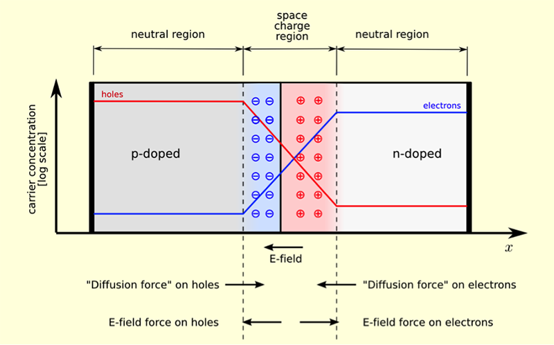
As we understand from the video, the p-n junction creates an internal electric field due to diffusion of charge carriers between two types of semiconductors (Figure 4.3). In this diagram, p-semiconductor is on the left, and n-semiconductor is on the right. p-semiconductor has excess of holes (positive charge carriers), as seen from the high position of the red curve on the left side, and the n-semiconductor has excess of electrons (negative charge carriers), as seen by the high position of the blue curve on the right side. At the junction region, which is defined as space charge region, there is a zone depleted of charge carriers: negatively charged impurities (shown as blue circles) "push away" the electrons in the n-semiconductor, and similarly, the positively charged impurities (shown as red circles) "push away" the holes in the p-semiconductor. This creates charge carrier separation. Also, in the depleted central region, co-presence of the negative and positive impurity atoms on both sides of the p-n boundary creates an electric field, which maintains that separation.
When light shines on the surface of the p-n material, photons excite electrons into conduction band, thus creating an electron-hole pair. If this happens in the n-doped side of the p-n junction, the newly excited electron is driven away from the junction, and the hole is swept across the junction to the p-doped side. This separation of the electron-hole pair is achieved by the action of the electric field in the space charge region. Then providing the external circuit (a wire) between the p- and n- semiconductors, we can initiate movement of the electron from the n-doped side to the p-doped side, where it recombines with a hole. This photo-induced electric current is the usable energy that can be harvested.
Please see the animated explanation to the light-induced current on the PVEducation website [8].
4.3. How PV performance is measured
4.3. How PV performance is measured
In the previous section, we understood how the photo-induced electric current is be generated at the p-n junction due to photovoltaic effect. How can we estimate the magnitude of that electric current?
To answer this question, first let us define the electron traffic across the band gap as generation or light-induced current (IL). Therefore, each photon absorbed is responsible for contributing one electron to the generation current inside the device. Hence, we can write:
where IL is light-induced generation current, q is the electron charge, N is the number of photons absorbed, and A is the surface area of the semiconductor exposed to light. Logically, we see that the more photons are absorbed, the higher the generation current. Also, the greater the area of semiconductor exposed to light, the higher the generation current. To be independent of the size of the cell, we can express this relationship in terms of current density (JL), which is current normalized by area:
For example, we can try to use this equation to estimate the current density of a photovoltaic device corresponding to the typical terrestrial light spectrum. Inputting values for electron charge (1.6 x 10⁻¹⁹ C) and number of photons in the absorbed range of spectrum for crystalline silicon (4.4 × 10¹⁷) to the above equation, we obtain:
(4.3)
This is the maximum current density that could be expected from a silicon cell, if there were no losses, and if all of the electrons were perfectly transferred through the external circuit. In reality, current losses take place, so the actual measured current density will be less than that ideal value (Markvart, 2000).
Next, let us see how the solar cell voltage can be estimated. The maximum voltage of a solar cell is determined by the semiconductor band gap. The electrostatic energy available due to separation of electrons and holes cannot exceed the band gap energy; otherwise, recombination would occur. The cell voltage (V) upper limit is therefore set by the following expression:
Numerically, the maximum voltage in volts is equal to the band gap energy in electron-volts. For example, the maximum voltage for a silicon solar cell is Vmax = 1.1 V
The same as with maximum current, the maximum voltage is never achieved practically because of losses and process limitations. However, in general, based on Eq. (4.4), the semiconductors with greater band gap indeed produce higher voltage (Markvart, 2000).
In summary: the maximum electric current of a solar cell is determined by the generation current, and the maximum voltage of a solar is determined by the material band gap.
In the above description, for simplicity, we assumed that all the photons (with energy above the band gap) reaching the surface are absorbed and transfer their energy onto electrons. This would be ideal and would give us ideal generation current. As a matter of fact, absorption of photos by semiconductors is material dependent and is controlled by the absorption coefficient. This is an important property to take into account, since it directly affects the charge carrier generation rate.
Reading Assignment
Absorption Coefficient / PVEducation.org [9]
Generation Rate / PVEducation.org [10]
The absorption coefficient role is well explained by these articles. Read through it to understand how the absorption coefficient affects the generation rate and how it changes with depth of the semiconductor material.
At this point, we have already recognized that the key parameters describing the performance of a solar cell are current density and cell voltage. We have looked into their origin - how they develop in the cell due to the photovoltaic effect, and looked at some factors that affect that process. Now, we will proceed to examination of the I-V characteristic (a.k.a. performance curve) and see how it is obtained and what different parts of this curve tell us about.
Using electric circuit notation, a solar cell can be represented by a diode, which represents the p-n junction.
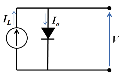
The current through the diode (Io) is the exchange current present when the element is in the dark. This is a small current compared to light-induced current (IL), which passes through the external load. The net current is the difference between the light and dark currents, or including Shockley diode equation:
where V is cell voltage, q is the charge of electron, k is the Boltzmann constant, and T is absolute temperature. This is the main equation that describes the relationship between voltage and current in the solar cell in operation. If we plot the cell voltage versus current (or current density), we will obtain the curve that generally looks like this (Figure 4.5):
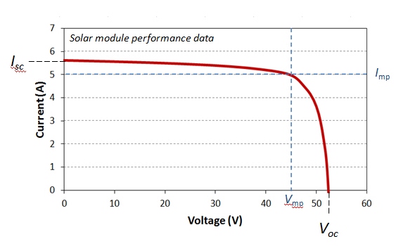
There are several important conditions to note on this curve. We see that at current being zero, the cell has the highest voltage. Because there is no current, the cell does not produce any work, but the voltage magnitude indicates the potential of the cell to do work. This is the open circuit voltage (Voc or OCV). The OCV is a very important characteristic of any galvanic cell (including solar cells), and it depends on the cell material. By re-arranging equation (4.5), and setting the net current to zero, we can express the open circuit voltage as follows:
At cell voltage set to zero, the cell current reaches some maximum limiting value, which is called short-circuit current (Isc). This is the kinetic parameter that shows the maximum current the cell is able to generate. It depends on the number of photons being absorbed by the material, optical properties of the cell and its size. You can imagine that if the sunlight intensity decreases for any reason, we will see a decrease in the short circuit current for a particular device. In an ideal case, the short-circuit current is equal to light-induced current: Isc = IL.
At any point on this curve (in Figure 4.5), we can define power output as follows:
At some point, the power will reach its maximum point, and the current and voltage corresponding to that point are defined as maximum power voltage (Vmp) and current (Imp):
These parameters are shown in the diagram in Figure 4.5. by blue dashed lines. They characterize the conditions when the cell produces the highest power output. This point is important because it is where the cell efficiency is usually determined.
At the maximum power point, we can also define the characteristic resistance of the cell (Rch). If the resistance of the external load is equal to Rch, then the maximum power is transferred to the load. The characteristic resistance can be determined from the Ohm's law:
The next term we need to define, when talking about the cell power output is the fill factor (FF). Please refer to the following reading to learn about the fill factor.
Reading Assignment
Fill Factor / PVEducation.org [11]
You are also welcome to try the FF calculators provided, which utilize the equations described on that website.
As you should have noted from the reading, the fill factor can be calculated as follows from the cell performance parameters:
The fill factor is a convenient metric to characterize the solar cell performance. For cells that work well, FF>0.7. Typical parameters of the single-crystal silicon solar cell are (Kalogirou, 2009):
Jsc = 32 mA/cm2
Voc = 0.58 V
Vmp= 0.47 V
FF = 0.72
Pmax = 2273 mW
Based on equation (4.10), the maximum power output of the PV system can be readily found using equation (4.11) if we know open-circuit voltage, short-circuit current, and fill factor.
The I-V characteristic is a convenient tool to explore the effect of various external variables on the cell performance. What is going to happen to a module output if temperature rises? What if light intensity drops because of the clouds? If cell is damaged or has bad contact with current collectors, how will it be reflected on the performance curve? Learn about these effects from the following readings:
Reading Assignment
Each of the following links will take you to a PVEducation web page that describes a certain effect on the solar cell performance. Read and take a note what events during the cell operation can cause these negative (parasitic) or positive effects (PVEducation.org).
Effect of Light Intensity [13]
Effect of Resistance [14]
Check Your Understanding - Question 4 (Essay)
Find the characteristic resistance of a solar cell that displays voltage of 40 V and current of 4 A at the maximum power point.
Rch =
Check Your Understanding - Question 5 (Essay)
Find the maximum power output of a PV system, if the open circuit voltage is 0.6 V, the short-circuit current is 0.32 A, and the fill factor is 0.8.
Pmax=
Check Your Understanding - Question 6 (Multiple Choice)
4.4. PV systems across scale
4.4. PV systems across scale
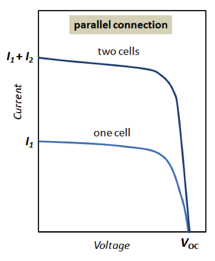
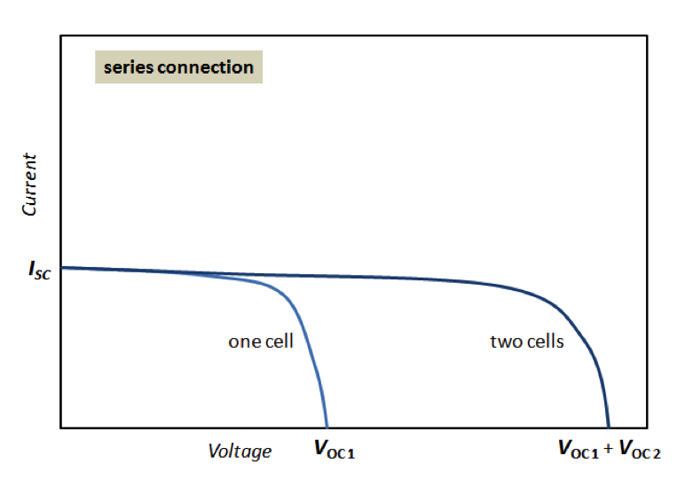
As we understand from the previous sections of this lesson, the electricity output of a single solar cell is relatively small, so cells need to be combined to provide enough power for any applications. Cells can be connected in series or in parallel. For example, when two identical cells are connected in parallel, the voltage of the system remains the same as for a single cell, but the current is doubled. When the same two cells are connected in series, voltage is doubled, while current remains the same. Examples of these combinations are shown in Figure 4.6.
To provide significant power output, solar cells are typically grouped into modules. A module is an engineered system consisting of multiple solar cells, wiring, frame, and glass. A module is a typical commercial stand-alone unit for solar cell applications. Each module can consist of a variable number of cells arranged in two-dimensional structure (Figure 4.7). In one direction, cells are connected in series to a branch. Then several branches are connected in parallel to complete a module (Figure 4.7).
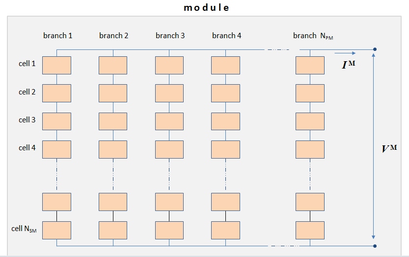
In Figure 4.7, the module voltage is denoted VM and module current is denoted IM (respectively, the single cell voltage and current will be denoted VC and IC in this presentation). This scheme depicts an example module that consists of NSM single solar cells connected in series and NPM parallel branches (subscript SM stands for series connection within module, and PM - for parallel connection within a module). The modules differ in design and may have variable number of parallel branches in order to deliver a certain current level. Many commercial modules may have simply one branch, i.e., all cells connected in series. To describe the electrical performance of a solar module, we can look at the model described in the reading material referred below. The model allows estimating the generated current and voltage of a module based on I-V characteristics of single cells.
Probing Question
Why would cells be normally connected in series, not in parallel, within modules?
If all the cells were connected in parallel, then the module would have an open circuit voltage of only 0.6 V, and a short circuite current of, for example 100 A. To transport this current, one would need an extremely thick cable. Furthermore, PV plants would need much higher voltages to be compatible with the grid.
The next step up the size scale will be grouping modules into an array (the same as it was done with grouping single cells into a module). A number of modules are connected in series within each branch, and then several branches are connected in parallel to form an array. Arrangement of modules in an array is shown in Figure 4.8.
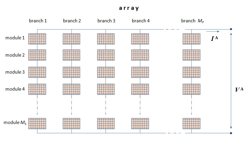
In Figure 4.8, each element is essentially a thumbnail of the arrangement shown in Figure 4.7. The total array current is IA depends on how many branches the arrays has, and the array voltage VA depends on how many modules are connected in one branch. Modules are common at the scale of distributed power generation (e.g. rooftops) and are also used as unit elements of larger solar facilities. Arrays are more typical for utility scale solar farms and plants. Next, you will learn how to calculate the voltage and current for large arrangements and thus to estimate the order of magnitude of power output.
Proceed to the following reading to become familiar with the basic models that describe the performance of solar modules and arrays.
Reading Assignment
Book Chapter: Kalogirou, S.A., Solar Energy Engineering. Processes and Systems. Elsevier, 2009, Chapter 9. "Photovoltaic Systems," pp. 482-486. (See E-Reserves via the Library Resources tab.)
Answer the following self-check questions to assess your learning of this section.
Check Your Understanding - Questions 7 & 8 (Multiple Choice)
Check Your Understanding - Question 9 (Essay)
What would be the voltage of the 5x5 module (consisting of the 5 parallel branches 5 single cells each connected in series), if each cell produces voltage of 0.4 V and current of 0.2 A?
V(module) =
I(module) =
4.5. Types of PV technology and recent innovations
4.5. Types of PV technology and recent innovations
There are different types of photovoltaics, some developed long ago, and others that are relatively new. Descriptions below provide a brief overview of a few well-developed PV materials. As you read through, please also open the links within each paragraph to get more information about each technology.
Monocrystalline silicon
Monocrystalline silicon solar cells are probably the oldest type of solar cells. They are made from pure silicon crystal, which has continuous lattice and almost no defects. Its properties provide for high efficiency of light conversion (typical ~15%; recent developments by SunPower boast improved efficiencies up to 22-24% ). Manufacturing of the Si crystals is rather complicated, which is responsible for high cost of this type of photovoltaics. Recent developments have decreased the total thickness of Si material used in monocrystalline cells to reduce cost. The monocrystalline silicon cells have a typical black or iridescent blue color. The monocrystalline silicon cells are believed to be very durable and last over 25 years. However, their efficiency will gradually decrease (about 0.5% per year), so replacement of operating modules might be needed sooner. The main disadvantages of the monocrystalline silicon panels are high initial cost and mechanical vulnerability (brittle). (Solar Facts and Advice: Monocrystalline Silicon [15], 2013)
Polycrystalline (or multicrystalline) silicon
Polycrystalline cells are made by assembling multiple grains and plates of silicon crystals into thin wafers. Smaller pieces of silicon are easier and cheaper to produce, so the manufacturing cost of this type of PV is less than that of monocrystalline silicon cells. The polycrystalline cells are slightly less efficient (~12%). These cells can be recognized by their mosaic-like appearance. Polycrystalline cells are also very durable and may have a service life of more than 25 years. The cons of this type of PV technology are mechanical brittleness and not very high efficiency of conversion. (Solar Facts and Advice: Polycrystalline [16], 2013)
Amorphous silicon (Thin-film)
Thin film photovoltaic cells are produced by depositing silicon film onto substrate glass. In this process, less silicon is used for manufacturing compared to mono- or polycrystalline cells, but this economy comes at the expense of conversion efficiency. Thin-film PV have efficiency of ~6% versus ~15% for single crystal Si cells. One way to improve the cell efficiency is to create a layered structure of several cells. The main advantage of the thin-film PV technology is that the amorphous silicon can be deposited on a variety of substrates, which can be made flexible and come in different shapes and therefore can be used in many applications. The amorphous silicon is also less prone to overheating, which usually decreases the solar cell performance. Amorphous silicon is most developed among the thin-film PV. (Solar Facts and Advice: Thin Film [17], 2013)
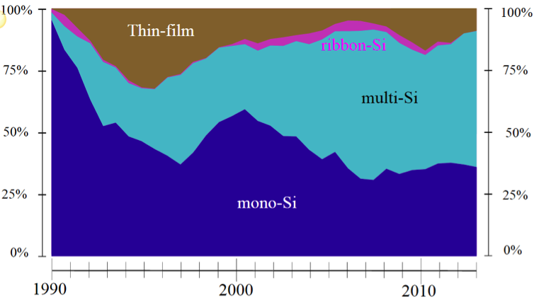
Figure 4.9, below, shows the trend of development and commercial implementation of different types of silicon PV technologies. There is no clear domination of a specific type of silicon substrate, as they all present a trade-off between cost and efficiency.
Cadmium Telluride, CdTe (thin-film)
CdTe PV are another kind of thin-film solar technology. It has become quite popular due to the lower cost per kW-hour. The best efficiency obtained with CdTe cells is around 16%. One of the advantages of the CdTe cells is that they capture shorter wavelengths of light than silicon cells can do. There are some environmental concerns related to the limited supply of tellurium and potential toxic impact of cadmium at the stage of CdTe panel disposal. Developing effective closed-loop recycling technologies can be a game-changing factor in favor of this technology. (Solar Facts and Advice: Cadmium Telluride [19], 2013)
Copper Indium Gallium Selenide (CIGS)
CIGS PV have become a popular new material for solar cells, as it does not contain toxic Cd, and has higher efficiency (just under 20%). At this moment, the CIGS are the most efficient among the thin-film PV technologies. While lab results confirmed high promise of this kind of photovoltaics, the mass production of CIGS proved to be a problem. The CIGS cells are manufactured by thin film deposition on a substrate, which can also be flexible (unlike the silicon cells). Similar to CdTe cells, the CIGS cells demonstrate good resistance to heating.
Polymer and organic PV
Organic materials are quite attractive since they can be involved in high-output manufacturing and also because they can be made in various thicknesses and shapes. These types of cells are relatively lightweight (compared to silicon cells). Also, they offer flexibility and relatively low fabrication cost. They, however, are much less efficient (about 1/3 of a typical Si cell efficiency) and sometimes prone to quicker degradation (shorter service life). More technical details about this type of PV technology can be read in this Wikipedia article: Organic Solar Cell [20].
These are a few most well-known varieties of PV technology, but there are many more innovations that are at the research and development stage. Breakthrough in new materials and cell design may be responsible for the growth of the PV industry in the upcoming decades. For this lesson discussion forum, you will be asked to do a search of recent innovations and share a quick synopsis of one that you believe especially interesting.
Summary and Activities
Summary and Activities
This lesson intended to provide you with the key concepts and terminology on the photovoltaic light conversion. It covers the basics of the photovoltaic effect and physical phenomena behind it, although it does not go into the depth of the science, but rather focuses on the practical understanding. Materials in this lesson also provide explanation to how the performance of the solar systems - cells, modules, arrays - is measured. Now, you should have an idea what the main parameters of the solar cell performance are, how to obtain them, and interpret them. You have learned how some of the key environmental parameters, such as temperature, light intensity, etc., affect the PV cell performance. The question of combining PV cells into bigger systems is discussed and illustrated with some examples, and we will return to the analysis of the larger-scale solar systems in Lesson 6, when more details will be given.
| Type | Description/Instructions | Deadline |
|---|---|---|
| Discussion Forum | Search recent research articles, press releases, and other sources for recent innovations in photovoltaic technology. Introduce this innovation at the discussion forum. In your post, try to deliver answers to the following questions:
|
Please submit your post by Sunday night. Responses are due by the following Wednesday. |
| Reading Quiz | Complete Lesson 4 Activity Quiz. | Please submit this assignment by next Wednesday night. |
References for Lesson 4
Markvart, T., Solar Electricity, John Wiley & Son, 2000.
Kalogirou, S.A., Solar Energy Engineering. Processes and Systems. Elsevier, 2009.
Honsberg, C. and Bowden, S., PVEducation.org, Photovoltaic Education Network., 2013.