Lesson 12: Semiconductors and Nanomaterials
Overview
Conventional integrated circuit technology is approaching its theoretical limits. Scientists and engineers are turning to materials which utilize quantum dynamics to push past the conventional materials limits. Nanoelectronics is a promising replacement possibility with a wide range of potential future applications. In this lesson, we introduce the basics of semiconductor technology, as well as the basics of going nano.
Learning Objectives
By the end of this lesson, you should be able to:
- Describe the four possible electron band structures for solid materials.
- For a p–n junction, explain the rectification process.
- Explain the concept of nanotechnology as it applies to materials.
Lesson Roadmap
Lesson 12 will take us one week to complete. Please refer to Canvas for specific due dates.
| To Read |
Read pp 323-347 (Ch. 15) in Introduction to Materials ebook The following required readings can be found in Canvas: |
|---|---|
| To Watch | Making Stuff: Smaller |
| To Do | Lesson 12 Quiz |
Questions?
If you have general questions about the course content or structure, please post them to the General Questions and Discussion forum in Canvas. If your question is of a more personal nature, feel free to send a message to all faculty and TAs through Canvas email. We will check daily to respond.
Energy Bands
Now that you have finished the reading for this lesson, I would like to review the four possible electron band structures for solid materials, as well as p-n junction electrical behavior. In addition, we will define nanotechnology and explore one possible application of nanotechnology which might allow for the continuing improvement in microprocessor speed in coming decades.
So, what happens when you try to shove a large number ( >1023) atoms together to make a solid? When atoms are separated, electrons will tend to occupy the lowest available discrete energy states. When atoms are brought together, the electrons are forbidden by the Pauli exclusion principle of having identical energy and quantum numbers. As shown in the figure below, as the atoms are brought closer and closer together individual allowed energy states start to spread in energy.
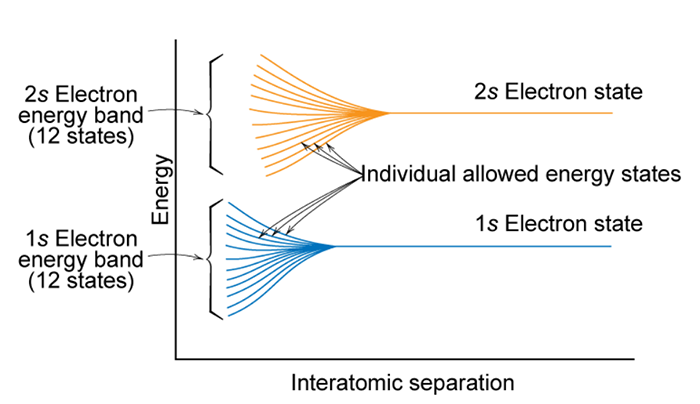
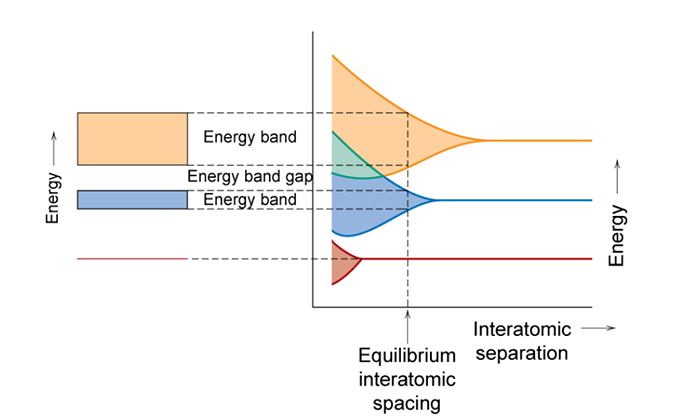
When you bring ~1023 atoms together to make a solid, the separation between the allowed energy states becomes indistinguishable (too small for us to measure). Since we can no longer distinguish the individual states, the allowable energy states form a range of energies that electrons can occupy. The ranges of allowable energies are referred to as bands. These bands are shown in the figure below. In this figure allowable energy levels are plotted versus interatomic separation. However, since there are too many levels to distinguish the band splitting is represented by a shaded region, instead of the individual levels shown in the previous figure. At the equilibrium interatomic spacing, i.e. the average distance between atoms in the stable material, the lowest energy states are not spread. These are 1s electrons of the atoms which are the electrons of the atom that are close to the nucleus of the atom. As such, they do not interact with the other atoms 1s electrons and do not have to spread in energy to satisfy the Pauli Exclusion Principle. However, for this atom at the equilibrium interatomic spacing depict in the figure below, the 2s and 2p states show clear energy splitting. The range of energy splitting for the 2s and 2p states are shown to the left of the graph as energy bands along with the 1s energy level.
Energy Bands (Continued)
As shown in the figures below, there are four possible band configurations.

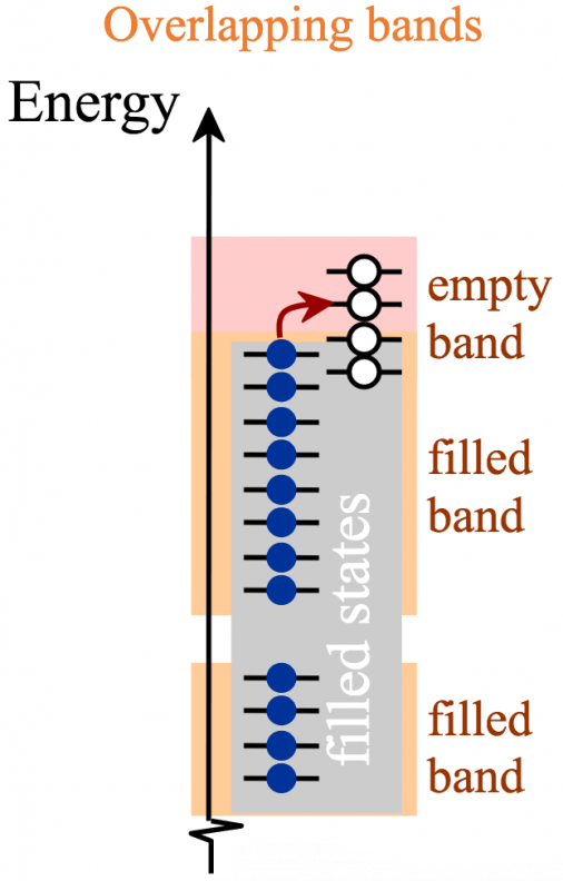
In the cases of (a) and (b), empty energy states are readily available and electrons (with a little bit of thermal energy) are able to speed through the material, similar to the cars pictured below.

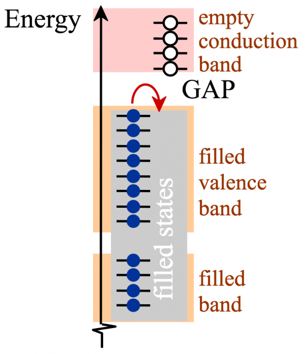
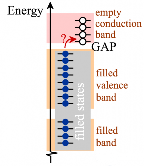
In cases of (c) and (d), insulator and semiconductor, the bands are completely filled and electrons have no mobility, because like the cars in the figure below, the electrons cannot move because there are no available open spaces to move to.

In the case of semiconductors, applying a voltage can boost the electrons across the gap. This would be like kicking one of the cars from the traffic jam over a medium to an unpacked highway. Thus, the semiconductor can be changed from being an insulator (off) to a conductor (on). We will look at one aspect of this behavior in the next section.
PN Junction
In a semiconductor, it is possible to dope the material with impurities that add electrons or holes to the semiconductors. (Think of the holes as adding more open spots on the freeway so that cars can move more easily.) When atoms with extra electrons are added, they are electron donors and the semiconductor is said to be doped to n-type. When atoms that accept extra electrons are added, they are electron acceptors and the semiconductor is said to be doped p-type. When p-type material is put together with n-type material you get the basic building block of the integrated circuit industry. Please watch the following video (10:36) on how p-n junctions work.
To Watch
We can find semiconductor p-n junctions in many places. They form part of electronic and optoelectronic devices such as solar cells that transform solar energy into electrical energy; light emitting diodes, known as LEDs; rectifier diodes and transistors. To understand what semiconductor materials are and how p-n junctions are fabricated, we need to dive into the atomic world.
Currently, the most well-known semiconductor is silicon. In a silicon crystal, each atom is bonded to its neighbors by four electrons forming covalent bonds. At low temperatures, these electrons remain in the covalent-bonds. When the temperature rises, some of the electrons in the bonds are able to gain thermal energy and escape. They are now free to move and to conduct electricity. At the same time, the broken bonds can be occupied by electrons from other bonds. For these electrons to move, no additional energy is required on average. This broken-bond or new state is termed hole and behaves as a particle of positive charge and mass.
Impurities can be introduced into the semiconductor, substituting atoms of a different atomic species for the silicon atoms. If the new atom has five electrons in its outer shell, four of them will replace the four electron-bonds of silicon. The extra electron will be loosely bound to the impurity. At room temperature, this fifth electron is liberated from its original atom, becoming a conduction electron. Consequently, the impurity acquires a positive charge. This may result in the number of electrons in the doped material exceeding the number present in a pure semiconductor. The number of implanted impurities can be controlled using the fabrication technology. A semiconductor containing these impurities is called an N-semiconductor, since it has negative charge carriers. The impurities are named "donor" impurities, since they donate electrons.
An impurity with only three electrons in its outer shell can also be used. The three outer electrons complete three of the four bonds. The fourth bond remains unoccupied. However, at room temperature the electrons from other bonds can move in to occupy this free space, creating a hole in the material and a negatively charged impurity. As in the previous case, the number of implanted impurities can be controlled using the fabrication technology. So, the number of holes in this doped material can be much greater than the number of holes in a pure semiconductor. A semiconductor of this type is called a P-semiconductor, because it has positive charge carriers, and these impurities are named acceptor impurities, since they accept an electron.
A p-n junction is a structure formed by neighboring regions with different dopings, p-type and n-type semiconductors. The p-n junction is a crucial part of many devices, such as, for example, the diode. If a positive voltage drop is applied between the p terminal and the n terminal of a diode, a large current can be observed experimentally. If we change the connectors and a positive voltage drop is applied between the n terminal and the p terminal, an extremely small current, negligible for most practical applications, is observed experimentally. The p-n junction shows this asymmetric behavior.
The current can flow in one direction but not in the other. This is a peculiar behavior, which enables a wide spectrum of applications in circuits OR which can be made use of in circuits in unique ways OR which can be very useful in circuits. To understand this particular feature of the p-n junction, we must consider two mechanisms that create an electric current: the diffusion mechanism and the drift mechanism.
One way to understand the diffusion mechanism is to imagine two sets of different-colored particles concentrated in two distinct zones. If the particles are free to move in different directions, their random motion tends to equalize their concentration in the whole volume. Diffusion is the physical mechanism which gives rise to free particles trying to occupy the maximum possible volume. The drift mechanism is a movement caused by an electric field. This electric field makes the positive charge carriers move in one direction, and the negative charge carriers in the other. If there is an electric field in a region of space, there will be an electric potential associated with it. The electric field points in the direction in which the electric potential decreases.
The varying electric potential acts as a barrier, preventing the charge movement. Its effects can be understood with the following analogy: let us consider a body moving at a certain speed in the gravitational field. If the body rises, it loses kinetic energy and gains potential energy. If the initial kinetic energy is not sufficient, the body will be unable to cross the barrier, but in the event that the initial kinetic energy is enough, the body may be able to surmount it and even have sufficient kinetic energy left to enable it to continue its movement. Similarly, the electric potential behaves like a barrier to the charged particles: it allows the particles to surmount it, whenever the kinetic energy is great enough. The process of fabricating a p-n junction begins with an n-type or p-type doped semiconductor into which the opposite type of impurity is introduced. To understand how this structure works and what physical processes take place in it, a didactic model is used. The model consists of a P semiconductor perfectly matched to an N semiconductor. The P semiconductor has a much higher hole concentration than the N semiconductor. Therefore, holes from the P region will diffuse into the N region. Similarly, electrons from the N region will diffuse into the P region.
The diffusion of electrons and holes creates a region depleted of free charge particles, leaving behind the ionized impurities from which these charged particles come. Thus, a region of positively ionized impurities and a region of negatively ionized impurities appear in the p-n junction. This special distribution of charges creates an electric field. The electric potential associated with this field acts as a barrier that prevents the displacement of the electrons and holes. Equilibrium is reached when the diffusion current equals the drift current.
The potential barrier is an obstacle for the diffusion current in the device. It is possible to reduce the height of this potential barrier by the application of an external voltage. This increases the electric current. By applying an external voltage from a battery, the height of the potential barrier in the junction is modified. If a positive voltage drop is applied between the P and N regions, the barrier height is reduced. A reduced barrier cannot prevent electrons and holes from diffusing across the structure. An electric current appears in the junction due to the diffusion mechanism. Under these conditions, the p-n junction is said to operate under forward bias.
If the voltage is reversed, and becomes greater in the N than the P region, the barrier height increases, preventing the electron and hole diffusion. The electric current is then negligible. In conclusion, the p-n junction can only conduct in a single direction, giving rise to a current which increases very rapidly when the potential barrier is significantly lowered. Besides being present in countless circuits and electronic components,p-n junctions can also be found in optoelectronic applications: in devices such as LEDs, photodiodes, and solar cells.
The origin of the light emitted from an LED can be found in the physical phenomenon of recombination. Recombination is a process where an electron and a hole are annihilated, releasing energy. In the case of certain materials, and under forward bias, this energy is emitted as light. The more electron-hole pairs recombine, the more intense this light is. The operation of the photodiodes and solar cells is based on the opposite physical phenomenon: generation. Thus, a photon can create an electron-hole pair, which by its movement can generate an electric current. To summarize, p-n junctions are ubiquitous in our environment, close and distant OR near and far. It seems unbelievable that such a simple device is so useful and affects so much in our lives.
Now let’s define nanotechnology and explore one possible application of nanotechnology which might allow for the continuing improvement in microprocessor speed in coming decades.
Introduction to Nanotechnology
Nanotechnology involves the control of atoms and molecules to produce materials in the size range of 1 – 100 nm, whose size or geometry dominates their material properties. Nanotechnology occurs in a size range were quantum mechanics dominate, but the materials are larger than a single atom. This size range is the range where single-atom behavior is transitioning to bulk material behavior. This allows for the tuning of properties to desirable results, which allows for the creation of designer materials. An example of this is gold nanoparticles. As shown in the figure below, nano-sized gold particles range in color from bright red, pink, purple, to blue, depending on the size of the nanoparticles.

So, how many atoms are we talking about when we say the material ranges from 1 to 100 nm in size?
A cube of 1 nm on a side would have around 100 atoms, while a cube of 100 nm on a side would have around 100 million atoms. That is quite a range. A former professor of this course, Dr. Peter Thrower, in his textbook Materials in Today’s World, calculated how many atoms would be on the surfaces of cubes of 1 nm (nanocube) and 1 cm (bulk cube). What he found was that in the nanocube, 60% of the atoms were on the surface of the cube. This was in stark contrast to the bulk cube, where only one out of 109 atoms were on the surface.
What does this mean chemically? Bulk gold is highly unreactive; it does not tarnish, it does not react with other metals, etc. It is so unreactive that it's possible to find gold in nature in its native state, gold nuggets. Nanogold, on the other hand, is extremely reactive. In bulk gold, the atoms are overwhelmingly non-surface atoms. These non-surface atoms have sufficient neighboring atoms to satisfy their bonds. In nanogold, most of the atoms are on the surface and possess unsatisfied bonds, which makes them extremely chemically reactive. This is a case where the size of the particle matters but also the geometry matters. In the case of nano gold, the geometry of possessing mostly surface atoms results in a chemically active material.
Introduction to Nanotechnology (Continued)
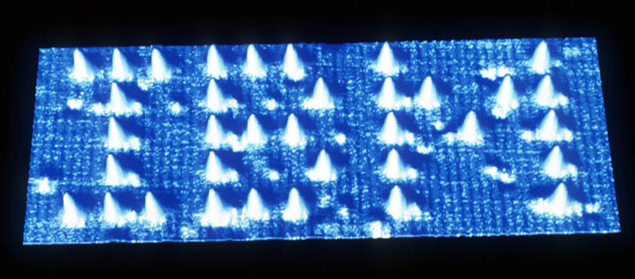
Nanotechnology, through the control of atoms and molecules, has the potential to create unique materials with wide-ranging applicability including the areas of medicine, smaller (faster) devices, self-assembled structures, and other designer materials applications. Nano materials are also allowing scientists to explore still unanswered fundamental materials questions. The field of nanotechnology is generally accepted to have been identified by Nobel laureate Richard Feynman during a futuristic talk entitled, "There’s Plenty of Room at the Bottom," in 1959. In that presentation, Feynman speculated about being able to write the entirety of the Encyclopedia Britannica on the head of the pin. On September 28, 1989, an IBM physicist, Don Eigler, became the first person to manipulate and position individual atoms. One example of his work is shown in the figure below utilizing 35 xenon atoms.
In the next section, we will look at how carbon nanotubes might allow for faster transistors in the future.
Moore's Law
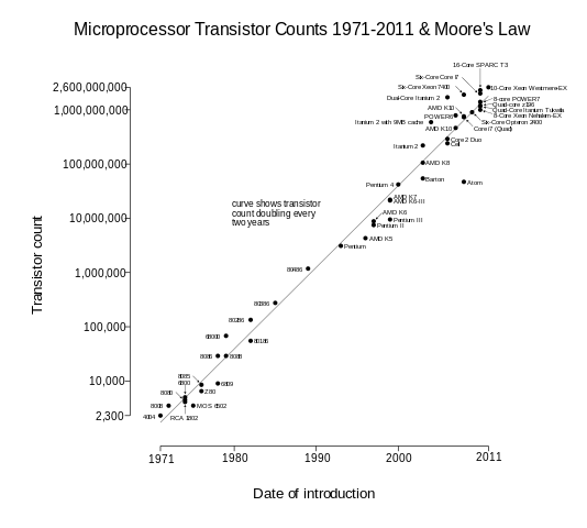
According to Wikipedia, "Moore's law is the observation that the number of transistors in a dense integrated circuit doubles approximately every two years." Gordon Moore made that observation in 1970, and as you can see from the figure below, it has been remarkably accurate over the many decades since.
But you cannot just keep making things smaller and smaller to make them faster and faster. At some point, you hit the limit of approaching zero and the fact that it becomes incredibly expensive to produce incredibly small feature sizes. As shown in the figure below, a leading trade magazine, IEEE Spectrum, has reported that transistors could stop shrinking in 2021.

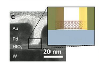
This will mean that faster computers will not be possible based on shrinking geometries. One potential approach, instead of increasing the density of transistors is the approach of making transistors faster by using carbon nanotubes. Electrons move much faster in carbon nanotubes than conventional semiconductor materials. A picture of a research carbon nanotube bridge is shown below.
Reading Assignment
Things to consider...
When you read this chapter, use the following questions to guide your reading. Remember to keep the learning objectives listed on the previous page in mind as you learn from this text.
- What are the four possible electron band structures for solid materials?
- What effect does the electron band structure have on the electrical conduction of a material?
- What is a p–n junction, and how does it rectify current?
- What are the concepts of nanotechnology as it applies to materials?
Reading Assignment
- Read pp 323-347 (Ch. 15) in Introduction to Materials ebook
- The following readings are available in Canvas.
- Pages 245 to 251 (Chapter 32) of Materials in Today's World by Peter Thrower and Thomas Mason.
- Pages 253 to 255 (Chapter 33) of Materials in Today's World by Peter Thrower and Thomas Mason.
Video Assignment: Making Stuff: Smaller
Now that you have read the text and thought about the questions I posed, take some time to watch the 53-minute NOVA video about how the latest in high-powered nano-circuits and microrobots may one day hold the key to saving lives. In "Making Stuff: Smaller," we see how making materials smaller has the potential for making vastly improved and tailored materials for future materials applications.
Video Assignment
Go to Lesson 12 in Canvas and watch the Making Stuff: Smaller video. You will be quizzed on the content of this video.
Summary and Final Tasks
Summary
As our understanding, and control, of materials at the nanometer scale improves, we are able to manufacture materials that are: tailored for specific tasks, designed to perform at the extremes of materials properties, or can utilize structure to enable properties not achievable before. Utilizing bottom-up, self-assembly, and other novel fabrication techniques, designer materials are becoming possible for everyday usage. In fact, superior materials are known today, but their utilization is hampered by our current inability to mass produce usable quantities economically. In this lesson, we looked at the basics of electronics, as well as some of the basics of nanoelectronics, which has the potential of being the electronics of the very near future.
Reminder - Complete all of the Lesson 12 tasks!
You have reached the end of Lesson 12! Double-check the to-do list on the Overview page to make sure you have completed all of the activities listed there before you take your final.