
4.2 P-N Junction
While photovoltaic effect readily takes place in a number of materials, the third step - separation of the charge carriers - is probably most tricky from the technical point of view. For example, in a regular silicon crystal, when absorption of a photon induces the release of an electron from the valence to the conduction band, a hole (positively charge locus) is formed in its place in the crystal lattice. Further, the excited electron and the hole can recombine to release heat. This is not what we want! So doping is often used to modify silicon structure. For example, boron (B) can be included into the structure in place of silicon. Because boron has valence of 3 (versus silicon valence of 4), there is a "gap" in the structure, which can accept an electron. This type of semiconductor, which has positive centers to accept electrons, is p-type semiconductor. Alternatively, silicon can be doped with phosphorus (P), which has valence of 5 and brings an extra valence electron, which is not involved in covalent bonds. This electron can be donated. This type of semiconductor is n-type semiconductor.
Thus, the p-semiconductors have excess of positive charge carriers, and the n-semiconductors have excess of negative charge carriers. If p- and n-types are put together, the interface between them will represent the p-n junction.
To understand how the p-n junction works, please watch the following video (10:36):
Video: The PN Junction. How Diodes Work? (10:36)
We can find semi-conductor PN junctions in many places. They form part of electronic and opto-electronic devices, such as solar cells, that transform solar energy into electrical energy, light-emitting diodes, known as LEDs, rectifier diodes, and transistors.
To understand what semiconductor materials are, and how PN junctions are fabricated, we need to dive into the atomic world. Currently, the most well-known semiconductor is silicon. In silicon crystal, each atom is bonded to its neighbors by four electrons, forming covalent bonds.
At low temperatures, these electrons remain in the covalent bonds. When the temperature rises, some of the electrons in the bonds are able to gain thermal energy, and escape. They are now free to move, and to conduct electricity. At the same time, the broken bonds can be occupied by electrons from other bonds.
For these electrons to move, no additional energy is required on average. This broken bond, or new state, is termed hole, and behaves as a particle of positive charge and mass.
Impurities can be introduced into the semiconductor, substituting atoms of a different atomic species for the silicon atoms. If the new atom has 5 electrons in its outer shell, four of them will replace the four electron bonds of silicon. The extra electron will be loosely bound to the impurity.
At room temperature, this fifth electron is liberated from its original atom, becoming a conduction electron. Consequently, the impurity acquires a positive charge. This may result in the number of electrons in the doped material exceeding the number present in a pure semiconductor.
The number of implanted impurities can be controlled using the fabrication technology. A semiconductor containing these impurities is called an N semiconductor, since it has negative charge carriers. The impurities are named donor impurities, since they donate electrons.
An impurity with only three electrons in its outer shell can also be used. The three outer electrons complete three of the four bonds. The fourth bond remains unoccupied. However, at room temperature, the electrons from other bonds can move in to occupy this free space, creating a hole in the material, and a negatively charged impurity.
As in the previous case, the number of implanted impurities can be controlled using the fabrication technology. So the number of holes in this doped material can be much greater than the number of holes in a pure semiconductor. A semiconductor of this type is called P semiconductor because it has positive charge carriers. And these impurities are named acceptor impurities, since they accept an electron.
A PN junction is a structure formed by neighboring regions, with different dopings. P type N type semi-conductors. The PN junction is a crucial part of many devices, such as for example, the diode. If a positive voltage drop is applied between the P terminal and the N terminal of a diode, a large current can be observed experimentally. If we change the connectors and a positive voltage drop is applied between the N terminal and the P terminal, an extremely small current, negligible for most practical applications, is observed experimentally.
The PN junction shows this asymmetric behavior. The current can flow in one direction, but not in the other. This is a peculiar behavior which enables a wide spectrum of applications in circuits. To understand this particular feature of the PN junction, we must consider two mechanisms that create an electric current. The diffusion mechanism, and the drift mechanism.
One way to understand the diffusion mechanism is to imagine two sets of different colored particles concentrated in two distinct zones. If the particles are free to move in different directions, their random motion tends to equalize their concentration in the whole volume. Diffusion is the physical mechanism which gives rise to free particles trying to occupy the maximum possible volume.
The drift mechanism is a movement caused by an electric field. This electric field makes the positive charge carriers move in one direction, and the negative charge carriers in the other. If there is an electric field in a region of space, there will be an electric potential associated with it. The electric field points in the direction in which the electric potential decreases. The varying electric potential acts as a barrier, preventing the charged movement.
Its effects can be understood with the following analogy. Let us consider a body moving at a certain speed in the gravitational field. If the body rises. It loses kinetic energy, and gains potential energy. If the initial kinetic energy is not sufficient, the body will be unable to cross the barrier. But in the event that the initial kinetic energy is enough, the body may be able to surmount it, and even have sufficient kinetic energy left to enable it to continue its movement.
Similarly, the electric potential behaves like a barrier to the charged particles. It allows the particles to surmount it, whenever the kinetic energy is great enough.
The process of fabricating a PN junction begins with an N type or P type doped semi-conductor, into which the opposite type of impurity is introduced. To understand how this structure works, and what physical processes take place in it, a didactic model is used. To model consists of a P semi-conductor, perfectly matched to an N semiconductor.
The P semiconductor has a much higher hole concentration than the N semiconductor. Therefore, holes from the P region will diffuse into the N region. Similarly, electrons from the N region will diffuse into the P region. The diffusion of electrons and holes creates a region depleted of free charged particles, leaving behind the ionized impurities from which these charged particles come. This a region of positive ionized impurities, and a region of negative ionized impurities, appear in the PN junction.
This special distribution of charges creates an electric field. The electric potential associated with this field acts as a barrier that prevents the displacement of the electrons and holes. Equilibrium is reached when the diffusion current equals the drift current.
The potential barrier is an obstacle for the diffusion current in the device. It is possible to reduce the height of this potential barrier by the application of an external voltage. This increases the electric current.
By applying an external voltage from a battery, the height of the potential barrier in the junction is modified. If a positive voltage drop is applied between the P and N regions, the barrier height is reduced. A reduced barrier cannot prevent electrons and holes from diffusing across the structure. An electric current appears in the junction due to the diffusion mechanism, under these conditions, PN the conjunction is said to operate under a forward bias.
If the voltage is reversed, and becomes greater in the N than the P region, the barrier height increases, preventing the electron hole diffusion. The electric current is then negligible. In conclusion, the PN junction can only conduct in a single direction, giving rise to a current which increases very rapidly when the potential barrier is significantly lowered.
Besides being present in countless circuits and electronic components, PN junctions can also be found in optoelectronic applications, in devices such as LEDs, photodiodes, and solar cells. The origin of the light emitted from an LED can be found in the physical phenomenon of recombination.
Recombination is a process where an electron and a hole are annihilated, releasing energy. In the case of certain materials and under forward bias, this energy is emitted as light. The more electron, hole pairs recombine, the more intense this light is.
The operation of the photodiodes and solar cells is based on the opposite physical phenomenon, generation. Thus, a photon can create an electron, hole pair, which by its movement can generate an electric current. To summarize, PN junctions are ubiquitous in our environment, close and distant. It seems unbelievable that such a simple device is so useful, and affects so much in our lives.
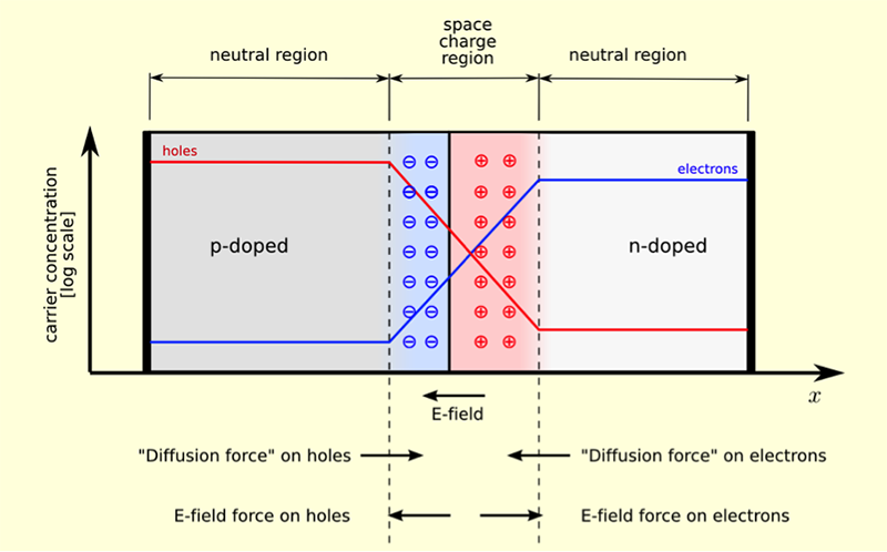
As we understand from the video, the p-n junction creates an internal electric field due to diffusion of charge carriers between two types of semiconductors (Figure 4.3). In this diagram, p-semiconductor is on the left, and n-semiconductor is on the right. p-semiconductor has excess of holes (positive charge carriers), as seen from the high position of the red curve on the left side, and the n-semiconductor has excess of electrons (negative charge carriers), as seen by the high position of the blue curve on the right side. At the junction region, which is defined as space charge region, there is a zone depleted of charge carriers: negatively charged impurities (shown as blue circles) "push away" the electrons in the n-semiconductor, and similarly, the positively charged impurities (shown as red circles) "push away" the holes in the p-semiconductor. This creates charge carrier separation. Also, in the depleted central region, co-presence of the negative and positive impurity atoms on both sides of the p-n boundary creates an electric field, which maintains that separation.
When light shines on the surface of the p-n material, photons excite electrons into conduction band, thus creating an electron-hole pair. If this happens in the n-doped side of the p-n junction, the newly excited electron is driven away from the junction, and the hole is swept across the junction to the p-doped side. This separation of the electron-hole pair is achieved by the action of the electric field in the space charge region. Then providing the external circuit (a wire) between the p- and n- semiconductors, we can initiate movement of the electron from the n-doped side to the p-doped side, where it recombines with a hole. This photo-induced electric current is the usable energy that can be harvested.
Please see the animated explanation to the light-induced current on the PVEducation website.